PCB Design And Layout Services
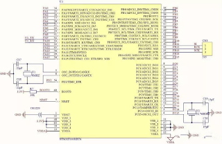
Printed circuit boards (PCBs) design services is one of the ways that we help our customers get to market faster as our engineering team has significant real world experience designing PCBs for performance and manufacturability.
Our 10 years of PCB manufacturing history allows us to quickly get customers full Gerber and drawing packages if you:
Require a PCB layout from design schematics you have created.
Have an existing design that needs to be updated, changed, or optimized for cost effective assembly.
Need a new PCB design, from concept (schematics/BOM) to creation (full PCB documentation).
Our team of engineers and CAD/CAM operators are available to discuss any project needs that our customer may have as we are fully licensed and utilize industry leading tools, including Cadence Allegro, Mentor Expedition, Mentor's PADS, Altium, Valor for DFM Analysis.
Our Capabilities Encompass The Full Design Flow From Start To Finish Including:
Micro BGA / Micro Via / Blind and Buried Vias
Rules Driven Designs
Schematic Capture
Library Development
Database Construction and Verification
Signal Integrity/Design Verification
EMI Checking
Full Document Package Creation
Electrical Engineering
We have the experience required to consistently meet the highest standards in the industry. Our experience spans multiple market segments, including Telecom, Datacom, Computer & Storage, Medical, Mil/Aero, Industrial, and consumer products.
Our expertise lies in High-Speed Circuitry Design up to 40GHz and Mesh Networking (Optical: OC-48, OC-192, T1, E1, and Infiniband).
Other capabilities include Thermal Engineering, Signal Integrity Analysis, Software and Firmware Design, including software integration and API design.
Digital/High-Speed and Analog Design Capabilities Include:
Circuit Design and Analysis
FPGA to ASIC Conversion
Component Analysis and Evaluation
Compliance and Value Engineering
Pulsed Circuits
Analog Circuit Simulation and much more!
Embedded Microprocessors and Chipsets for Power PC, Intel x86, TI DSP, Mellanox, Broadcom and various other chipsets used in Server, Telecom, Industrial, and Commercial market segments
Mechanical Engineering
Our Engineers have 10 years experience in Mechanical Engineering. We are capable of supporting any part of the product life cycle across multiple market segments. We utilize leading CAD platforms such as AutoCAD Inventor, SolidWorks, and Pro/ENGINEER Wildfire.
Our Mechanical Engineering Capabilities Include:
Packaging, Enclosure, and Industrial Design
Product/System Architecture
Detailed Mechanical Design
Stress Analysis (FEA) Shock/Vibration Simulation
Thermal Simulation
Material and Component Selection
Solid Modeling
PCB Linkage DFM / DFA and Cost reduction
Epec Can Provide:
Concept Sketches/Rendering
Product Specifications
Mock Ups
3D Rendering
Full Documentation
For over 10 years Epec has been your reliable PCB manufacture. From prototype to production runs our engineers can support you in all your PCB needs 24/7. Why look elsewhere, from the simplest single sided PCB to HDI, sequential laminated multi-layers with multiple blind and buried vias we've got you covered. Via in pad, silver filled, copper filled, epoxy, conductive, non-conductive via fill, Aluminum, RF, ENEPIG, our specialty is customer service.
As we continue to expand our PCB supply chain we have one goal in mind, to provide our valued customers what they need when they need it. Supporting domestic 1, 2, 3 day quick turns, 5 day turns from Asia and our guarantee to satisfy.
SI Analysis
Our SI experts have years of experience in pre-design and post-design verification and analysis. This experience and expertise, combined with powerful state-of-the-art software, helps ensure your design will work the way you expect it to the first time and all the time. Although we can customize services to meet your unique needs, we have included a list below of the services we provide.
SI Analysis Capabilities Include:
Up Front SI Risk Analysis
Pre and Post Route Simulations
Frequency Domain and Time Domain Modeling
3D Via Field Modeling and Optimization
Optimization of AC Coupling Cap Launches
Optimization of Connector Launches
Infiniband, PCIe (Gen 1 & 2), XAUI link Analysis
IEEE 802.3ap KR Compliance to 10 Gbps
StatEye Time Domain Analysis
DDR2 and DDR3 Optimization
Crosstalk and Timing Analysis
Detailed SI CAD Guidelines Generation
Real Time SI Support Throughout the CAD Layout Process
PCB design
We have a deep experience in designing the most up-to-date circuits, which we do with the leading design software (Altium, Cadence, Zuken, Mentor Graphics) independent of platform.
We are proud to design more than 50 circuits a year, most of which are complex high-speed digital PCBs.
The circuits designed by us comply with IPC standards and are cost effective to manufacture.
Besides circuit design, we undertake to develop products from the idea to production, providing the background based on engineering, embedded software development and project management.
We organise 2/3-day courses on high-speed circuit design.
Schematic

Designing a circuit diagram means more than just drawing the circuit in the CAD system, it often includes selecting the main components and developing the detailed technical specifications.
Very often, contradicting requirements (on price, availability, manufacturability) have to be complied with during the design phase, that is why we focus on continuous consultation with our clients to be able to make optimal decisions.
Besides having our own parts library, we prepare unique parts libraries as well.
PCB layout
Manufacturability, industrial standards and cost effective implementation are amongst the main aspects taken into consideration when designing PCBs. We provide the 3D model of the PCB in STEP and 3D PDF formats for the mechanical engineering of the product.
Circuits consisting of FPGA and multi-core processors are implemented on 10+ layers using mikrovia technology and fineness under 100 micrometre, taking into account the limitations of the chosen manufacturing technology.
In case of designing high-speed (1G-10G) digital circuits, optimal signal transfer is provided by creating a unique layer order (stackup), controlled wiring of the impedance, timing analysis and IBIS simulation.
SPICE and IBIS simulation
As part of the product design process, we create the proper layer order before starting to wire the PCB. For high-speed signal wires and memory interfaces, we use IBIS simulation to optimise impedances, reflections, cut-offs, crosstalks and timings.
For multi-gigabit interfaces, the transfer channel is characterised using IBIS-AMI models and 3D simulation in HyperLynx.
We use SPICE simulation to control the correct operation of the analogue stage.
If you need a PCB design, please email to service@pcbsky.com


The information you've provided is useful because it provides a wealth of knowledge about Online Vlsi Institutes that will be highly beneficial to me. Thank you for sharing that. Keep up the good work.
ReplyDeleteThis is very educational content and written well for a change. It's nice to see that some people still understand how to write a quality post.
ReplyDeleteGet the Best Institute for AutoCAD Training Course in Delhi
Looking for the Best Institute for JAVA Training Course in Delhi
Python Training Course, Certification Institute in Delhi
Complete SAP Training Course with Placement Guaranteed
I have read all the comments and suggestions posted by the visitors for this article are very fine, we will wait for your next article so only. Thanks!
ReplyDeleteSoftware Testing Training, Courses in Delhi,NCR
Complete MS Office Training Course , Institute in Delhi
C&C++ Training Course with Placement Support
DATA ANALYTICS Training with Excel Course in Delhi
Thank you for this detailed analyzation over PCB layout services .
ReplyDelete